Description:
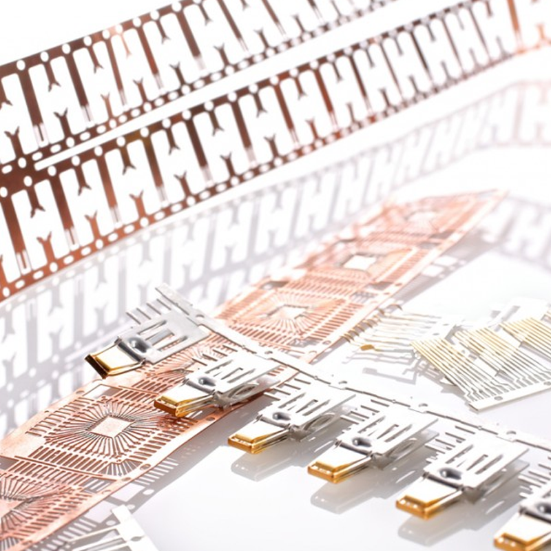
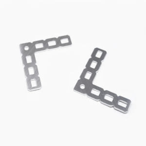
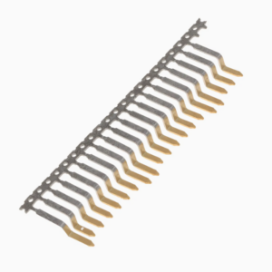
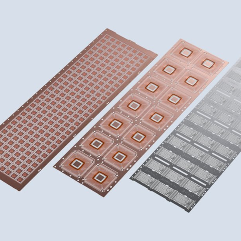
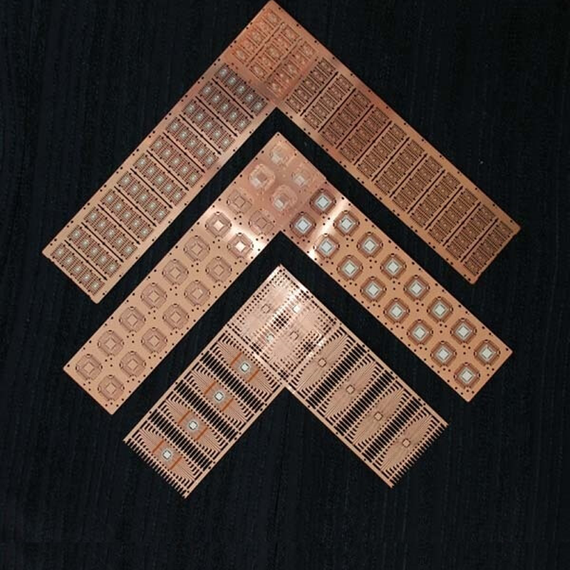
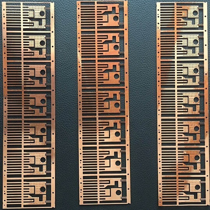
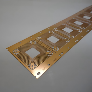
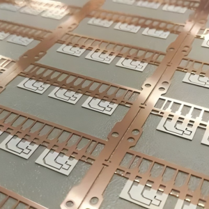
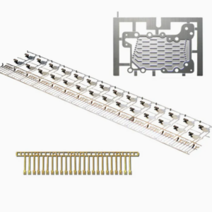
Our gold-plated stamped lead frames for the integrated circuit (IC) industry are meticulously manufactured using high-quality copper or brass. These lead frames are produced through precision stamping processes, followed by an advanced gold plating technique that enhances conductivity, corrosion resistance, and overall durability. Designed specifically for semiconductor packaging, our custom lead frames ensure optimal electrical performance and long-term reliability. We offer comprehensive OEM services, providing tailor-made sizes, surface finishes, and design specifications to meet the exact requirements of your project. Whether you need high-precision stamping or specialized coatings, our expertise ensures that every lead frame meets the highest industry standards.
Characteristics:
| Item | Details |
| Place of Origin | Xiamen, China |
| Brand Name | OEM |
| Service | OEM Services |
| Processing Type | Metal Stamping |
| Size | Customized Size |
| Application | Semiconductor Package |
| Frame Thickness | Custom |
| Color | Custom |
| Size Tolerance | ±0.025 mm |
| Material | Copper |
| QC Control | 100% Inspection |
Post-Processing Treatments:
- Passivation: This specialized chemical treatment forms a protective oxide layer on metal surfaces, significantly enhancing corrosion resistance. Passivation is particularly beneficial for components exposed to challenging environmental conditions, providing long-lasting durability and performance.
- Silver Plating: A thin layer of silver is electroplated onto the base material to significantly improve electrical conductivity, corrosion resistance, and solderability. This treatment is commonly employed in high-performance electronics and semiconductor applications where reliable electrical connections are crucial.
- Nickel Plating: Electroplated nickel is applied to enhance the surface hardness and wear resistance of components, offering superior protection against corrosion. This process is ideal for industrial and automotive applications where parts are subjected to high stress and harsh conditions.
- Tin Plating: Tin is electroplated onto metal surfaces to improve corrosion resistance and enhance solderability, making it particularly useful in electronic components. The tin coating prevents oxidation and ensures reliable electrical performance in a variety of applications, especially in environments where moisture exposure is a concern.
Production Process:
- Material Selection and Preparation: Premium-grade copper or copper alloys are carefully chosen for their superior electrical conductivity and durability. The selected material is precisely processed to the required thickness and dimensions, ensuring it is suitable for high-performance applications.
- Metal Stamping: Using state-of-the-art progressive dies, the copper material is subjected to high-precision stamping. This process forms the intricate patterns and components of the lead frame, ensuring exact dimensional accuracy and adherence to design specifications.
- Etching: After stamping, the lead frame undergoes an etching process to refine its edges and surface. This step is crucial for improving the frame’s surface profile, ensuring optimal bonding for plating and enhancing overall functionality in semiconductor packaging.
- Gold Plating: A uniform layer of gold is applied to the stamped lead frame through an advanced electroplating process. This gold plating enhances the lead frame’s electrical conductivity, provides excellent corrosion resistance, and ensures long-term reliability in high-performance semiconductor applications.
- Inspection and Quality Control: The final product undergoes comprehensive inspection procedures, including visual examination, dimensional analysis, and functional testing. These strict quality control measures guarantee that each lead frame meets exacting industry standards and tolerances.
- Final Packaging: Once inspected, the lead frames are meticulously packaged to safeguard them from any potential damage during transportation. The packaging is designed to maintain the integrity of the product, ensuring it arrives at the client in optimal condition.
Factory Overview:
Our manufacturing facility is fully equipped with a wide array of advanced machinery to ensure the highest standards of production quality. We operate 25 punch presses with capacities ranging from 25 to 300 tons, along with precision wire EDM machines, grinding equipment, welding tools, and polishing stations. Additionally, our ultrasonic cleaning systems ensure thorough and precise cleaning for all components.
To further enhance the durability, appearance, and performance of our products, we offer a comprehensive suite of metal plating services, including electroplating, zinc plating, nickel plating, chrome plating, and anodizing. These processes are carefully controlled to deliver superior finishes and long-lasting protection.
With our advanced production capabilities, stringent quality control protocols, and cutting-edge plating technologies, we consistently deliver products that meet or exceed industry standards, ensuring exceptional performance and reliability for our clients.




Reviews
There are no reviews yet.