Metal stamping is a vital part of the semiconductor manufacturing process, and its impact on the functionality and reliability of semiconductor devices cannot be overstated. As professionals in the metal fabrication and stamping industry, we at Topmetalstamping understand the significance of producing high-precision components that meet the stringent demands of the semiconductor industry. Metal stamped parts, such as custom metal bellows, wafer handling components, test sockets, and lead frames, are essential for ensuring that semiconductor devices operate with high performance and longevity.
In the rapidly evolving world of semiconductor technology, precise metal components are the backbone of many applications. These parts must be engineered with extreme accuracy and consistent quality, as even the smallest discrepancy can lead to malfunction or failure in sensitive electronic systems. With over two decades of experience in metal stamping, Topmetalstamping offers specialized solutions tailored to the needs of this high-tech industry, ensuring each component performs flawlessly in demanding environments.
Custom Metal Bellows
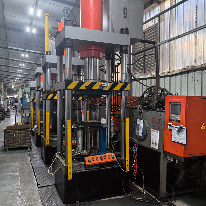
Custom metal bellows are integral to a wide range of semiconductor manufacturing equipment. These bellows provide flexibility and are critical in applications requiring a hermetic seal. At Topmetalstamping, we use advanced deep drawing and stamping processes to create bellows that meet tight tolerances and perform under high stress. Bellows are particularly useful in machinery that requires the movement of gases, as they maintain the integrity of sealed environments while accommodating mechanical motion.
The manufacturing of metal bellows involves a meticulous process that ensures both durability and flexibility. The use of deep drawing techniques allows the metal to be stretched into the desired shape without compromising its strength. For applications that demand the utmost precision, Topmetalstamping offers several options of bellows, including welded, formed, and electroformed versions. Each type is designed to meet specific performance requirements, whether it’s strength, flexibility, or high precision.
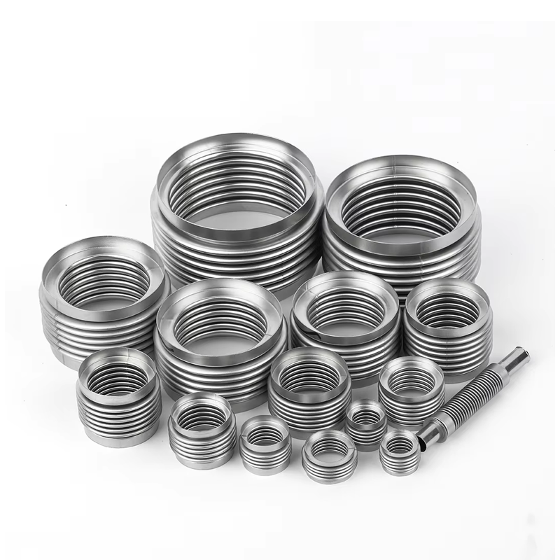
Within semiconductor operations, custom metal bellows are used in the following key applications:
- Slit valves: These regulate gas flow with pinpoint accuracy in semiconductor equipment.
- Orientors: They ensure proper positioning and handling of wafers during processing.
- Actuators: High-precision movement control in machinery.
- Gate valves: Control the flow of gases and liquids in vacuum systems.
- Flexible couplings and beam lines: Accommodate movement and direction changes in sensitive machinery.
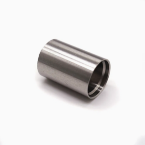
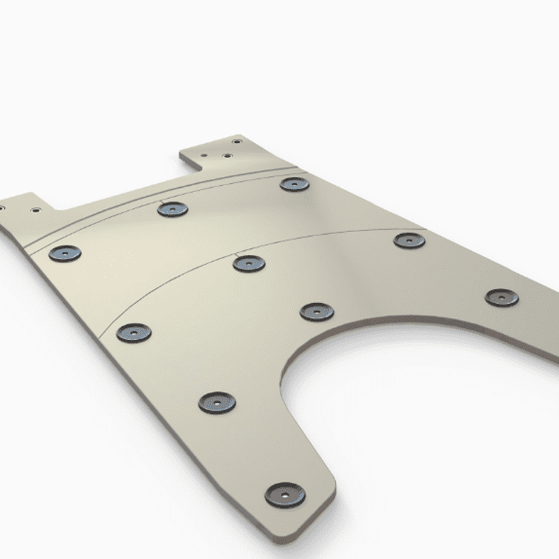
Precision Wafer Handling Components
Wafer handling components are indispensable in the semiconductor industry, where precision and contamination control are paramount. At Topmetalstamping, we craft wafer handling parts with extreme care, ensuring that each component meets the necessary standards for interaction with sensitive semiconductor wafers.
Wafer handling involves a variety of components, including:
- End effectors: These are part of robotic arms used to handle wafers while minimizing the risk of contamination and damage.
- Cassettes: These secure and transport wafers safely through various stages of the manufacturing process.
- Aligners: These components ensure that wafers are properly aligned for precise material deposition or etching.
- Elevators and indexers: Facilitate smooth movement of wafers within the system, reducing manual handling and potential for error.
Manufacturing techniques for wafer handling components focus heavily on precision. Topmetalstamping employs advanced stamping methods, such as progressive stamping, to produce parts with high accuracy, which is essential for the sensitive nature of semiconductor wafer handling. These processes allow for the production of complex shapes with tight tolerances, crucial for ensuring that the wafers are processed correctly, without risk of damage or contamination.
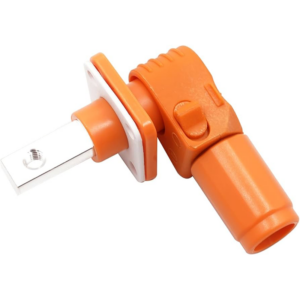
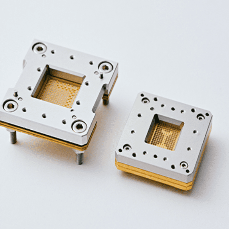
Test Sockets
Test sockets are critical to the semiconductor industry, as they provide the interface for testing integrated circuits (ICs) before assembly into final products. These sockets allow semiconductor manufacturers to conduct electrical tests under real-world conditions, ensuring that ICs will perform correctly in the end device. At Topmetalstamping, we specialize in manufacturing test sockets using cutting-edge metal stamping technology that ensures high precision and reliability.
Test sockets are made with tight tolerances to ensure a secure and stable connection between the testing equipment and the IC. Stamping provides a high-speed production method that maintains the precision needed for efficient testing. Some test sockets also require secondary processes like laser cutting or injection molding for specific features.
Common types of test sockets include:
- Pin Grid Array (PGA): For ICs with a grid of pins on the bottom, used to test multiple pins simultaneously.
- Surface Mount Technology (SMT): Designed for ICs with surface-mounted leads, allowing easy connection to testing equipment.
- Ball Grid Array (BGA): Used for ICs with solder balls, providing a reliable testing interface.
- Dual In-line Package (DIP): Typically used for legacy ICs.
- ZIF (Zero Insertion Force): These sockets minimize mechanical stress during IC insertion and removal.
With Topmetalstamping, semiconductor manufacturers can rely on precision-crafted test sockets that ensure accurate and efficient testing, helping to minimize the risk of faults in final products.
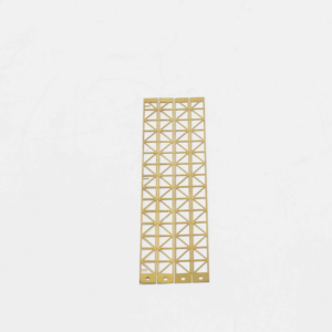
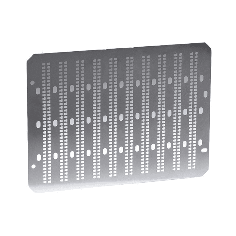
Lead Frames
Lead frames are essential in the packaging process of semiconductor devices. They provide mechanical support and electrical connectivity between the integrated circuit (IC) and external components. These frames are necessary for the longevity and durability of semiconductor devices, ensuring that they maintain functionality throughout their lifecycle.
Manufacturing lead frames typically involves the use of metal stamping and etching techniques, which are ideal for creating the fine patterns and intricate designs required for semiconductor packaging. Topmetalstamping uses advanced stamping and progressive stamping techniques to create lead frames that meet the specific needs of various semiconductor packages. We can also employ deep drawing techniques to form features that are tailored for particular design specifications.
Types of lead frames include:
- Dual In-line Package (DIP): Used for ICs with two rows of pins.
- Surface Mount Device (SMD): For ICs designed for surface mounting.
- Chip-on-Board (COB): Used when the IC is directly attached to the PCB.
- Ball Grid Array (BGA): Support for ICs with solder balls.
- Small Outline Package (SOP): For small devices with closely spaced leads.
Lead frames play a vital role in industries such as:
- Semiconductor Packaging: Ensuring secure connections and mechanical support.
- Consumer Electronics: Used in microchips for electronics like smartphones and computers.
- Automotive: Vital for chips that control safety systems and infotainment in vehicles.
- Medical Devices: Crucial for devices requiring high precision and reliability.
- Industrial Equipment: Used in chips powering sensors and machinery.
Conclusion
In conclusion, metal stamped parts like custom metal bellows, wafer handling components, test sockets, and lead frames are indispensable in the semiconductor industry. These components play a pivotal role in ensuring the functionality, reliability, and efficiency of semiconductor devices. If you’re looking for high-precision stamped components that meet the stringent requirements of the semiconductor industry, Topmetalstamping is your trusted partner.
Our expertise in metal stamping, combined with advanced manufacturing technologies, allows us to deliver components that meet the highest standards of quality and performance. Whether you need custom solutions or standard parts, Topmetalstamping is committed to providing tailored solutions that meet your specific needs.
Contact Topmetalstamping today to learn more about how our precision metal stamping can support your semiconductor manufacturing processes. Let us help you enhance your products with the reliability and precision they need.